

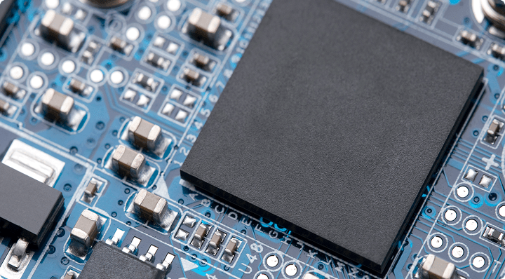
HBM / Advanced Packaging
Internal inspection for stacked packages, bonding interfaces, and hidden voids in advanced semiconductor packaging.
VoidDelaminationBonding failure
Applications
HBM and advanced packaging are placed first for global semiconductor relevance, while batteries and industrial inspection remain visible as expansion markets.
Internal inspection for stacked packages, bonding interfaces, and hidden voids in advanced semiconductor packaging.

Wafer-level acoustic imaging for internal defects that optical inspection cannot expose.

Inspection support for modules where bonding quality and thermal reliability matter.

Non-destructive review of internal battery structures and delamination-prone interfaces.
Inspection for compact devices where physical sectioning is slow, risky, or destructive.

Acoustic inspection for internal discontinuities in composite structures.
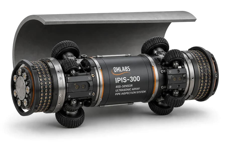
Industrial inspection direction for pipe and infrastructure assets with custom sensing systems.